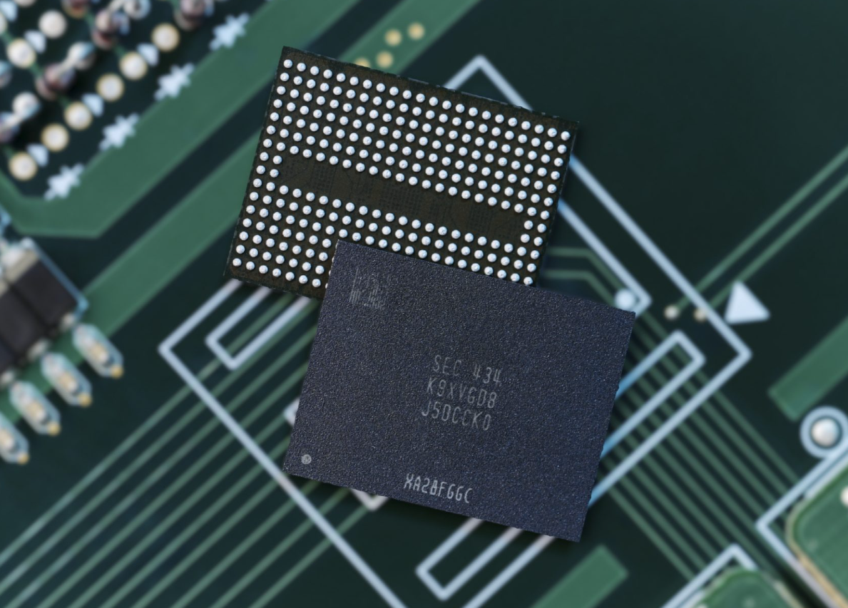
Samsung, one of the largest technology companies, is working on a new type of storage technology that will let people save even more data on their devices. This new memory, called “400-layer V-NAND,” will be faster, hold more information, and last longer than what is currently available. Samsung plans to release it in 2026.

What is V-NAND and why does it matter?
V-NAND is a special type of memory that stores data in many layers, stacked on top of each other like floors in a tall building. The more layers, the more data can be stored in the same amount of space. Right now, the manufacturer’s latest memory chip has 280 layers, but the next one will have 400 layers—an increase of 43% in just one generation! This large boost in layers will mean much higher storage in a similar-sized chip.
Samsung will use a new method called “Bonding Vertical (BV) NAND” to build this 400-layer V-NAND. The South Korean company isn’t stopping here. It is aiming for even more layers, hoping to reach up to 1,000 layers by around 2027. This would make memory chips even more powerful and useful for smartphones, computers, and data centres.
How will Samsung build this new memory?
This method is different from their older design, known as Circuit on Periphery (CoP), where the circuits that control the memory are placed on top. With the BV NAND method, Samsung will create the storage layers and the circuits separately and then join them vertically.
This change not only helps stack more layers safely but also keeps the chip strong and reduces the risk of damage while building. Other companies, such as YMTC and Kioxia-Western Digital, have already adopted similar approaches, and Samsung is now joining this trend.
This process allows Samsung to achieve up to 60% more “bit density.” Bit density refers to the number of data points that can be stored within a certain space. Higher bit density means their chips can store more data without getting larger.
What about future goals?
Samsung has ambitious plans for its memory technology. Beyond the 400-layer V-NAND coming in 2026, Samsung aims to create chips with up to 1,000 layers, possibly by 2027. This would mean a 2.5 times increase in layers compared to the current generation, making devices even more powerful and able to process more data at faster speeds.
Samsung’s plans for faster DRAM
In addition to V-NAND storage, Samsung is working on making its DRAM faster and more efficient. DRAM is another type of memory used to help devices quickly access data. Samsung plans to introduce a new type of DRAM in 2027. This new DRAM will be based on a very small technology called “0a nm” (less than 10 nanometers) and will use something called Vertical Channel Transistor (VCT) technology. With VCT, Samsung will be able to stack DRAM in 3D layers, which should make it more powerful while reducing interference between cells.
The development of this new DRAM will happen in stages: Samsung will begin with “1c nm” DRAM in 2025, move to “1d nm” DRAM in 2026, and reach the advanced “0a nm” technology in 2027.
What does this mean for everyday users?
These advances in memory technology mean that future smartphones, computers, and other devices will be able to store and process much more information. This will make everyday tasks like taking pictures, streaming videos, or using apps even faster and smoother. Additionally, this new memory will be helpful for big companies that need to store large amounts of data, like data centres and cloud services.
In summary, Samsung’s next-gen V-NAND and DRAM technologies are pushing the limits of what memory chips can do. With the new 400-layer V-NAND and future plans for 1,000 layers, Samsung is leading the way in creating memory that will allow our devices to be faster, store more data, and last longer than ever before.
For tech-related news, click right here.